

Laser Application: How to Realize the Soldering Requirements of PCB and FPC Gold Finger
Laser Application: How to Realize the Soldering Requirements of PCB and FPC Gold Finger
FPC is a flexible printed circuit board (Flexible Printed Circuit Board, referred to as FPC), which is a circuit board made of PI (polyimide) film as the base material and laminated with copper foil. Compared with PCB rigid printed circuit boards, FPC circuit boards have the advantages of free bending, folding and winding. When assembling a product, the FPC can be arbitrarily arranged according to the layout of the internal space of the product like the wire, so that the components can be arranged arbitrarily in the three-dimensional space, and the connection between the wire and the circuit board can also be cancelled. Therefore, FPC The electronic products can be miniaturized and refined, and the reliability of the products can be greatly improved.
FPC has been widely used in mobile communication products, laptop computers, consumer electronic products, aerospace, military electronic equipment and other fields.
One of the main features of FPC is that it can realize circuit connection. There are mainly two existing connection methods. One is to use a connector to connect. Although it is convenient to use a connector to connect, it requires a lot of space for installation, and the insertion is unstable. The disadvantage of high cost makes it only used in some PCB boards with large space and high hardness.
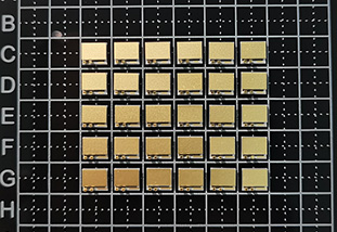
The usual circuit connection is still by welding. To weld FPC, it is necessary to process the gold finger. The FPC gold finger is an area where only copper foil is left after removing the double-sided PI. Its ultra-thin thickness plus The ductility of copper is not very good, which makes the gold finger end of the FPC extremely fragile. Therefore, the current processing technology generally adds a PI layer to the blank of the gold finger to enhance the flexibility and tensile strength of the gold finger end. However, the shear stress resistance of FPC and the difficulty of welding and welding yield have not been greatly improved.
The FPC gold finger in the prior art also has the following disadvantages:
1. The ability of FPC welding position to resist stress is very low, and many problems such as breakage, gold finger detachment, and welding position falling off are easy to occur in the production and transportation process and the production process;
2. The process difficulty of the FPC welding process increases, and it is easy to cause virtual welding to lead to product failure;
3. The stress limit that the FPC welding position can bear is very small, which reduces the quality and life of the assembled product.
So can FPC gold fingers be laser welded?
The answer is yes, in order to solve the problems existing in the prior art, a laser soldering technology for gold fingers of FPC is provided, which dislocates the copper foils on both sides of the gold fingers at the welding end of the FPC, which reduces the processing difficulty of the welding process. , reducing the possibility of gold fingers breaking during welding, improving the product welding yield; enhancing the stress strength of the FPC welding position, reducing the FPC welding position in the production process. The quality of the assembled product and the product life.
To realize the welding requirements of fpc gold finger and pcba connection components:
1. The height of the pins on the welding surface of the plug-in components is 1.5 to 2.0 mm. The SMD components should be flat on the board surface, the solder joints should be smooth without burrs and slightly arc-shaped, and the solder should exceed 2/3 of the height of the soldering end, but should not exceed the height of the soldering end. Less tin, spherical solder joints or solder covering patches are all bad;
2. Height of solder joints: The height of solder climbing pins should not be less than 1mm for single panel, not less than 0.5mm for double panel and need to penetrate tin.
3. The shape of the solder joint: it is conical and covers the entire pad.
4. Solder joint surface: smooth and bright, no black spots, flux and other debris, no spikes, pits, pores, exposed copper and other defects.
5. Solder joint strength: fully wetted with pads and pins, without false soldering and false soldering.
6. Cross section of solder joints: The cutting feet of the components should not be cut to the solder part as much as possible, and there is no cracking phenomenon on the contact surface between the pins and the solder. There are no spikes and barbs at the cross section.
7. Needle seat welding: The needle seat needs to be inserted into the bottom board, and the position is correct and the direction is correct. After the needle seat is welded, the bottom floating height should not exceed 0.5mm, and the seat body should not be skewed beyond the silk screen frame. The rows of needle seats should also be kept neat, and no dislocation or unevenness is allowed.
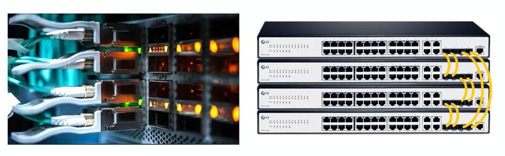 How to Select Optical Modules for Switch Stacking?
 Cold Core Technology achieves successful mass production of non-airtight Micro-TEC
 GSA: The latest deployment of LTE and 5G networks worldwide
 Vertical integration tempers high-quality, differentiated fiber laser solutions